Effect of Fixtures on Deformation and Warpage
Study on the Effect of Fixtures on Deformation and Warpage of the Double-Sided Flexible Printed Circuit Board Through Reflow Using DIC
Pradeep Lall, Kartik Goyal
Auburn University
NSF-CAVE3 Electronics Research Center
Department of Mechanical Engineering
Auburn, AL 36849
Tele:(334) 844-3424
E-mail:
Â
Abstract – Flexible electronics provide new design options not afforded by rigid electronics in a variety of applications including wearable electronics, robotics and automotive systems. However, the processes for the manufacturing of complex electronic assemblies using fine-pitch components are not as well developed as those for rigid electronics. The lack of structural rigidity of flexible printed circuit cards requires the use of fixtures or palletes for component placement and subsequent reflow. In addition, mechanisms are needed to compensate for the deformation and warpage of the flexible substrate and components during assembly. In this paper, two different fixture options have been presented for the manufacture of flexible circuits. The first fixture option includes the use of a pallete with tensioners. The second fixture option includes the use of vacuum fixture during reflow of the flex circuit assembly. The deformation of the flex circuit assemblies during reflow has been studied using a combination of low-speed high resolution cameras in conjunction with digital image correlation. The double-sided board used for the experiment is of BGA  –
– combination with dummy components, A-PBGA–
 mm-
mm- mm and A-CABGA–mm-
 mm. Firstly, warping of the flexible circuit with only PBGA on the front side was studied, then CABGA was placed on the back side using the pick and place machine, and warping was studied again, both using DIC. Two low speed Point Grey Cameras were used to capture many frames of flexible circuit going through every stage in reflow and a DIC software Vic 3D
  was used to get the warpage measurements. Both of the warping data has been presented in this paper and compared with the results in rigid circuit boards.
Keywords – Digital Image Correlation (DIC), flexible circuit, warpage, BGA package, flexible circuit fixtures.
INTRODUCTION
    Since the last few decades, flexible electronics have been replacing rigid electronics, and are found in everything from as common as notebooks, mobile phones, to as sophisticated as military and avionics systems. This transition itself is major evidence of a major technical revolution. Although the flexible circuit technology evolved recently, it has long been envisioned by famous researchers at the turn of the 20th century. Flexible Printed Circuits (FPCs) provides whole range of benefits that surpasses and cannot be achieved from rigid Printed Circuit Boards (PCBs), such as more design freedom, dynamic flexing, and many more. To meet ever increasing demand for innovative electronics and designs, flexible circuit technology has been branching out significantly from its initial role of wire replacement.
    Warpage is defined as the out-of-plane displacement a package or a PCB experiences due to CTE (coefficient of thermal expansion) mismatch between different materials, processing conditions, and package architecture. Many studies have been performed in the past to examine the warpage that occurs in electronic packages mounted on a rigid board during solder reflow , , . Warpage, when in excess, may result in many problems, if not addressed, such as open connections, loss-of-coplanarity, which significantly influences the reliability and performance of electronic packages and boards. Since the electronic assemblies have a greater tendency to experience warping at high and low temperatures, warpage during a solder reflow is a key factor to consider to do reliability analysis of FPCs. Shadow Moiré or Moiré interferometery, a conventional, non-contact full optical method was used initially to measure out-of-plane displacement to learn the warpage behavior of electronic packages . Later, Digital Image Correlation (DIC) was introduced by Park et al , a non-contact, non-optical method to measure the deformation and strain fields due to its robustness and simplicity. DIC, a state-of-art technique has been used by many researchers in various scenarios, such as transient-shock, drop impact, thermal analysis of BGA packages, deformation of a solder joint of BGA assembly, to get full-field deformation and strains , , , . The effect of package architecture, material properties, and process conditions which greatly affect the warpage has also been studied in detail for a Package-on-Package module using FEA . But there are not many open literatures present for the warpage in FPCs.
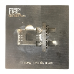
    Flexible circuits, because of their flexibility, they require fixtures to keep them flat during fabrication process. However, FPCs still warp and show deformation when put through reflow oven as temperature increases. In this article, two fixtures have been exploited: a pallete with four fixed pins and two tensioners, and a vacuum fixture. Both of the fixtures are shown in Fig.  –
–  .
.
 Test Vehicle Description
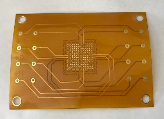     The test vehicle is designed to investigate the temperature effect on the flex circuit and understand the warping behavior during solder reflow. The double-sided flex circuit is shown in Fig.
      –
–  . The circuit is designed to accommodate two surface-mount BGA components: A-PBGA256-1.0mm-17mm and A-CABGA144-1.0mm-13mm. Both of the BGAs are daisy-chained mechanical dummy samples shown in Fig.
  .Package specifications are shown in Table 1.


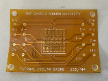
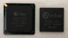
Figure 5. Dummy Packages. PBGA (left) and CABGA (right).
Table 1. Packages Specifications
|
Part Description |
I/O count |
Pitch |
Ball Height |
Body Size |
Ball Matrix |
|
A-PBGA256-1.0mm-17mm |
|
|
|
|
|
|
A-CABGA144-1.0mm-13mm |
|
|
|
|
|
 mm
mm mm
mm mm
mm    The double-sided flexible circuit consists of a base film of polyimide of  m, one copper layer on both sides of the film of
  m, top and bottom film thickness of
  m and
m and  m respectively, and ENIG (Electroless nickel immersion gold) surface finish of
  . The flex circuit of
  x
x  has a total thickness of
  mm. The cross section of the flex circuit is shown in Fig.
  .
.


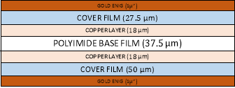
Figure 6: Flexible Circuit Composition.
   The warpage of the flex circuit with BGA components is studied using 3D digital image correlation.
- Principle of DIC
    The basic principle of DIC requires taking digital images of the specimen surface from a CCD camera before and after deformation and iteratively, computing the motion of each image point in a subset by comparing both images using computer program that is developed based on well-established algorithms and interpolation schemes to obtain the desired displacement and strain fields. Fig.  shows a schematic of the DIC principle. The computer program Vic 3D is widely used and accepted by many researchers to perform DIC. However, there are certain requirements to be met to get an accurate displacement or strain field from DIC, such as: (1) the specimen surface must have a random gray intensity distribution or speckle pattern; (2) the CCD cameras should not be moved while taking the digital images, and must be calibrated before running DIC; (3) the subset size should be carefully selected before running DIC. It should be large enough that contains sufficient distinctive pattern and small enough that can accurately approximate deformation field using subset shape function. Study on subset size selection has been studied by many researchers , .
    Vic D, when the above mentioned requirements are met, performs the correlation using pre-defined algorithms and provides us with the full-field displacement and strain values.
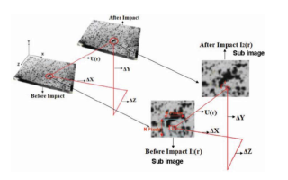
Figure 7[3]. DIC Schematic.
EXPERIMENT
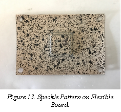
    DIC, whether it is D or D, provides the displacements and strains acting on a specimen surface. The main difference is that 3D provides out-of-plane displacements while 2D provides in-plane displacements. It further demands the surface should have a random intensity pattern or speckle pattern to get the most accurate results. In this study, the most conventional technique used in obtaining the speckles, the spray paint method is used. A layer of white paint is sprayed on the surface and black paint is sprinkled onto it to create a fine speckle pattern. An image of a pattern is shown in the Fig  .
.
D DIC is performed by correlating digital images: reference and deformed, from two CCD cameras focusing on the specimen surface. Studies have been performed on the different parameters, such as the angle between the two cameras, facet size, facet step, which affects the displacement/strain results .
    Flexible circuits tend to bend and requires the use of a pallete or a fixture to keep them flat while surface-mounting the components and during reflow. In this study, two types of fixtures have been used: pallete with tensioners, and a vacuum fixture.
- Pallete
The pallete, as shown in Fig.  consists of two tensioners and four fixed pins which are used to keep the circuit flat during all the processes. To perform DIC on the back surface of the circuit which has CABGA
  , the pallete has a pocket in which front package, PBGA
  can be flushed in while surface mounting and reflow of CABGA .


Figure 8. Pallete with Tensioners.
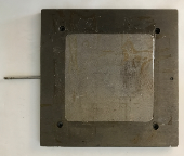
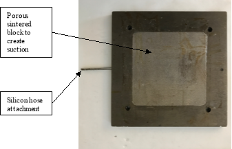
- Vacuum Fixture
A vacuum fixture, shown in Fig.  consists of a porous sintered block of stainless steel which when attached to a vacuum pump with a silicone hose, creates a suction force which keeps the flexible circuit flat during the reflow process. This fixture, due to lack of a pocket to flush PBGA package, cannot be used to perform DIC on CABGA . Therefore, DIC was only performed on the front side of the circuit, which is PBGA .

- Test Procedure
In order to keep the flexible circuit flat, both of the fixtures have been used during all the stages of assembly: pre-baking, placement, speckle pattern, reflow.
    The test procedure follows the following steps:
Pre-bake
Flexible circuits, made of polyimide layer are very hygroscopic in nature and readily absorb moisture when kept at room temperature. Therefore, before placement of components, flexible circuits are pre-baked at  for hours to remove any moisture from the circuits.
Placement of BGA Packages
First, PBGA is placed on the circuit using standard pick and place machine. A stencil printer was used to place SAC  solder on the circuit. During placement of the solder and package, flex circuit needs to be flat to perfectly mount the component and to avoid any resistivity errors. Therefore, both, pallete and vacuum fixture were used to keep the circuit flat during this process. For CABGA , only pallete was used because of the pocket to flush in PBGA , which vacuum fixture lacks in. Fabricated circuits on the pallete are shown in Fig.
  .
.
    From the Fig. , it can be seen that the size of the sintered stainless steel block is greater than the size of the flex circuit. Therefore, Kapton tape was used as shown in Fig.  to cover the exposed area and the through-holes on the circuit to direct the vacuum suction force on the circuit and on the area where package is placed.
Figure 10. Fabricated Packages on the Pallete.
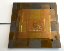
Figure 11. Kapton Tape on Vacuum Fixture.
    Packages were also placed, both sides on the rigid circuit boards, shown in Fig.  .
.

Speckle Pattern
    3D DIC demands the surface to have an intensity pattern or speckle pattern to track points on the specimen surface to obtain displacements and strains. Conventional spraying method has been used to create artificial speckle pattern. White paint is sprayed on the circuit surface, and then the black paint is sprinkled onto the top to create a distinctive pattern. An example of a speckle pattern on a flexible circuit board is shown in Fig. .
Camera Calibration
To generate useful and accurate displacement and strain results, calibration of the cameras must be performed before starting the reflow process. Calibration is a key process and has a major influence on the performance of the whole system. DIC calibration provides us with two types of parameters: Intrinsic and Extrinsic. Intrinsic parameters indicate the internal optical characteristics of the camera such as focal length of the lenses, position between the lenses, sensor center. Extrinsic parameters indicate the external characteristics between camera and the specimen surface such as the distance between the lens and surface, translation vector, distance between the cameras.
    To achieve a sub-pixel accuracy, a  calibration grid or calibration target, with known distance between the points, as shown in Fig.
  is used to calibrate the stereo system in Vic D software. An error of less than ___ was achieved in all of the experimental tests.
    Detail description on the camera calibration can be found in literature .
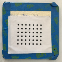
Figure 14. Calibration Target.
Reflow Process
After creating speckle pattern and calibrating the cameras, reflow profile was selected, with the maximum temperature going up to  for the flexible board and
  for rigid boards, and the process was started. Reflow profiles for the flexible circuit board and rigid circuit board are shown in Fig.
  and Fig.
  respectively. At the same time cameras were also turned on to start the recording. Features of Vic D software were used to make sure that the cameras starts recording at the same time the reflow process starts. Test Setup for the reflow process can be seen in Fig.
  .
.


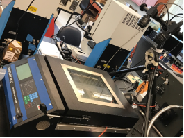
Figure 15. Test Setup.
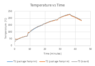
Figure 16. Reflow Profile (Flexible Board).
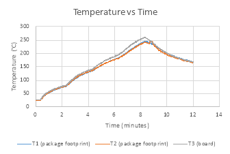
Figure 17. Reflow Profile (Rigid Board).
RESULTS
Warpage study has been performed on the double-sided flexible printed circuit board using D DIC using two fixtures to keep the flex circuit flat: pallete with tensioners, and a vacuum fixture. Multiple warpage results for both the fixtures have been performed to check if the repeatability in the warpage occurs. DIC was also performed on the double-sided rigid circuit boards to compare the warpage results between flexible and rigid boards.
     Full-field displacements are plotted for the points along the diagonal at the maximum temperature and the z-displacements has been plotted as a function of temperature as it increases to the maximum temperature. Warpage values are only considered till the reflow zone of the profile.
- Pallete
     Warpage results of both sides of the flexible circuit with packages PBGA and CABGA using pallete with tensioners have been presented. Reflow of PBGA was performed first, which implies there is no package on the bottom, while reflow of CABGA was performed second, which implies there is package on the bottom, and furthermore the package is PBGA .
    Fig.  –
– shows the comparison of two warpage tests displacements for the points along the diagonal at the maximum temperature in x, y, and z-direction and near the edges of the package versus the temperature increase for the front side of flexible board.
    Similarly, Fig.  –
– shows the warpage results for the back side of the flexible board when there is package on the bottom of CABGA .
- Vacuum Fixture
    Warpage results of the flexible board for only one side, with PBGA have been presented. Due to lack of pocket to flush in package as compared to the pallete, reflow and DIC of CABGA was not performed on the vacuum fixture.
    Fig.  –
– shows the comparison of warpage tests performed on the front side of the flexible circuit.
- Comparison with Rigid Boards
    Warpage measurements of the double-sided flexible circuit board have been compared with the rigid circuit board in this section.
    The rigid boards are of the same configuration with two packages. DIC was performed on both sides of the board and the warpage has been plotted in Fig.  –
–  for the front side of the board, and Fig.
  –
–  for the back side when there is a package on the bottom.
    The negative values presented in below warpage results should not be interpreted as the contraction of material. The negative value signifies that the point at which displacement is extracted, experiences displacement in negative direction from the origin defined in reference frame, which is at the start of the reflow process. Before starting the DIC process, origin in a reference frame is specified to be at the center of the package.
Results-I(a): Flexible Circuit Board (PBGA  on Pallete
     The graphs below shows the warpage in a flexible circuit for the points along the diagonal from bottom-left to top-left and near the edges of PBGA .
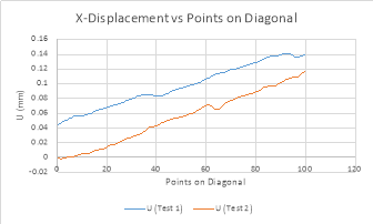
    Fig. –  shows the increase in x and y displacement as points on diagonal move from bottom-left to top-right. Fig.
  also shows the increase in z-displacement initially till the point where tensioners come in place which leads to decrease in warpage as they work to keep the circuit flat and decreases to the minimum to the point where tensioners are. Fig.
  – shows the increase in z-displacement as the temperature increases and reaches to the maximum in the reflow profile. The maximum displacement in Fig. – can be seen in the middle, which it should be because of the fixed pins and tensioners on the corners of the board.

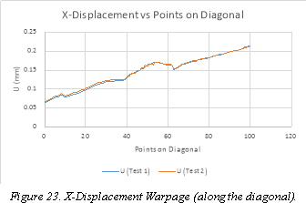
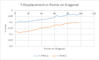 Figure 19. Y-Displacement Warpage (along the diagonal).


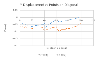
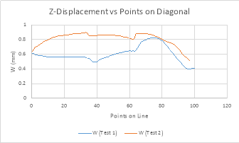
Figure 20. Z-Displacement Warpage (along the diagonal).


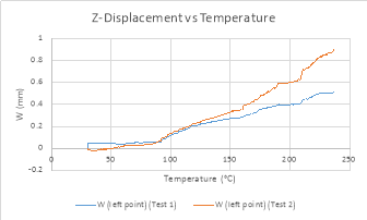
Figure 21. Z-Displacement Warpage (Left Edge of Package).

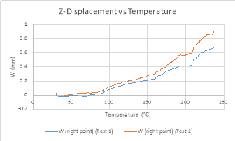 Figure 22. Z-Displacement Warpage (Right Edge of Package).
Results-I(b): Flexible Circuit Board (CABGA ) on Pallete
    The graphs below show the warpage results for the back side of the flexible circuit board for the points along the diagonal and near the edges of the package.
     Fig. shows the increase in x-displacement for points along the diagonal and maximum on the tensioners, which are pulling the circuit to the right to keep them flat. For y and z-displacements in Fig.
      –
–  , trends look different as compared to the front side because of the bigger package in the
bottom and the second-time reflow of PBGA , which affects the warpage of CABGA . Similar argument can be hold for the decrease in z-displacement in Fig.  – , which is, because of the bigger and heavier package on the bottom which leads to decrease in z-displacement till the 2nd pre-heat zone and as the temperature goes higher, temperature dominates the weight of the package and the warpage increases.


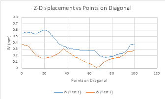
Figure 25. Z-Displacement Warpage (along the diagonal).

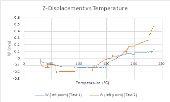
Figure 26. Z-Displacement Warpage (Left Edge of Package).

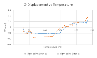
Figure 27. Z-Displacement Warpage (Right Edge of Package).
Results-II: Flexible Circuit Board (PBGA on Vacuum Fixture
    Warpage of the flexible circuit with the use of vacuum fixture is also studied. Only PBGA reflow was performed on the vacuum fixture due to the lack of pocket to flush in the package for the reflow of CABGA as compared to the pallete. Full-field displacements are plotted versus points along the diagonal and versus the increase in temperature.
    Fig. –  shows the increase in x and y displacement at the maximum temperature for points along the diagonal. Fig.
  shows the increase in z-displacement in Test , and not much increase in Test . The reason for the different displacement trend can be argued because of the unpredictability of the flexible circuit during the use of vacuum fixture. The trend in z-displacement in Fig.
  – is similar to the displacements with the pallete, increases as the temperature reaches to the maximum. Although, maximum displacement is higher in the case of vacuum fixture as compared to the pallete, which rather came unexpected.

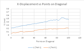
Figure 28. X-Displacement Warpage (along the diagonal).

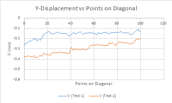
Figure 29. Y-Displacement Warpage (along the diagonal).

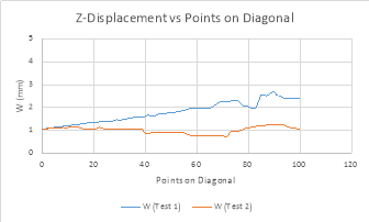
Figure 30. Z-Displacement Warpage (along the diagonal).


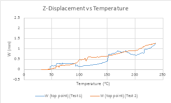
Figure 31. Z-Displacement Warpage (Top Edge of Package).

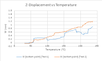
Figure 32. Z-Displacement Warpage (Bottom Edge of Package).
Results-III(a): Rigid Circuit Boards (PBGA )
    Warpage results for the rigid circuit boards are presented in below figures. Rigid circuit boards have the same configuration as compared to the flexible circuit board. Initially, reflow and DIC was performed on PBGA followed by the reflow and DIC of CABGA .


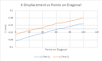     Fig. –
      shows the increase in x and y displacement at
the maximum temperature along the diagonal. Fig.  shows the z-displacement trend, which does not have much change along the diagonal. Fig.
  – shows a decrease in displacement initially and then increases as the temperature increases to the maximum. Many reasons may have contributed for the initial, very small decrease in displacement such as the FR- material property, CTE mismatch between package and the board.


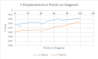
Figure 34. Y-Displacement Warpage (along the diagonal).


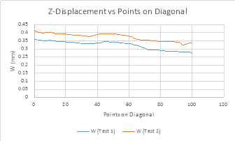
Figure 35. Z-Displacement Warpage (along the diagonal).
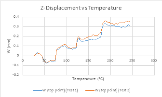
Figure 36. Z-Displacement Warpage (Top Edge of Package).
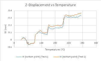
Figure 37. Z-Displacement Warpage (Bottom Edge of Package).
Results-III(b): Rigid Circuit Boards (CABGA )
    The figures below shows the warpage results for the back side of the rigid circuit board (CABGA ) with a package on the bottom (PBGA ).

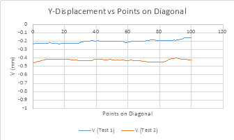

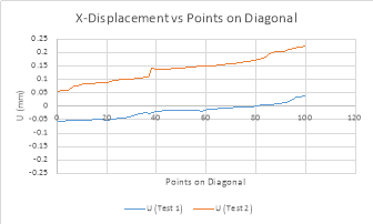     Fig. shows the increase in x-displacement for the points along the diagonal at the maximum temperature. Not much change is seen in the y and z displacement along the diagonal as shown in Fig.
      –
–  .Increase in z-displacements near the edges of the package as the temperature increases are shown in Fig.
  – .Bottom package does not seem to have much effect in the case of the rigid circuit boards as compared to the flexible circuit board, which can be seen in Fig. – .

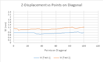
Figure 40. Z-Displacement Warpage (along the diagonal).


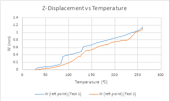
Figure 41. Z-Displacement Warpage (Left Edge of Package).
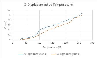
 Figure 42. Z-Displacement Warpage (Right Edge of Package).
SUMMARY AND CONCLUSIONS
    This study focuses on the warpage of the double-sided flexible circuit board which occurs during the process of solder reflow and the effect of fixtures on the deformation of flexible board using DIC. DIC is a well-established, commonly used technique which provides the full-field displacement of a surface having a random gray-intensity distribution or speckle pattern. Warpage results of double-sided flexible and rigid printed circuit boards with BGA packages, PBGA and CABGA have been presented.
    For the flexible circuit board, two fixtures have been used: pallete with tensioners; and a vacuum fixture. Warpage results from the vacuum fixture provided with more z-displacement as compared to the pallete, which was rather unexpected to notice. From the warpage results of CABGA , it can be seen that the bottom package, PBGA , leads to decrease in the z- deformation because of the weight and second-time reflow of it, but there was hardly any effect of PBGA in the case of rigid circuit boards. A point to be noted is in all of the warpage results, negative displacement does not imply that the material is contracting. All it signifies is the point at which displacement is extracted, experiences a negative displacement from the origin defined in reference frame, which is at the start of the reflow process and DIC.
    This study allows the user to understand and learn the warpage behavior of the double-sided flexible printed circuit board and how the fixtures, which are required to keep them flat, affect its deformation. Furthermore, it also allows the user to compare the deformation or warpage of flexible board with the rigid boards. Understanding the warpage behavior is very crucial in electronics packaging industry. This paper is written in hope of helping packaging industry to learn the warpage of flexible boards and meet ever increasing demand of innovative electronics.
ACKOWLEDGMENTS
The research results presented in this paper are based on projects supported by industrial members of NSF-CAVE3 Electronics Research Center at Auburn University, Alabama.
REFERENCES
- M. Amagai and Y. Suzuki, “A study of package warpage for package on package (PoP),” 2010 Proceedings 60th Electronic Components and Technology Conference (ECTC), Las Vegas, NV, USA, 2010, pp. 226-233.
- F. Yen, E. Chen, J. Y. Lai and Y. P. Wang, “The Introduction of Warpage Improvement Guidelines for BGA’s Performance within SMT Temperature Profile,” 2008 3rd International Microsystems, Packaging, Assembly & Circuits Technology Conference, Taipei, 2008, pp. 278-282.
- P. Lall, K. Patel and V. Narayan, “Model for Inverse Determination of Process and Material Parameters for Control of Package-on-Package Warpage,” in IEEE Transactions on Components, Packaging and Manufacturing Technology, vol. 5, no. 9, pp. 1358-1375, Sept. 2015.
- Han, Y. Guo, and H.C. Choi, “Out-of-plane displacement measurement of printed circuit board by shadow moiré with variable sensitivity,” Proceedings of the 1993 ASME International Electronics Packaging Conference. 1993, Vol. 4-1. pp. 179-185.
- S.B. Park, R. Dhakal, L. Lehman and E. Cotts, “Measurement of deformations in SnAgCu solder interconnects under in situ thermal loading,” Acta materialia. May. 2007, vol. 55, no. 9, pp. 3242-3260.
- P. Lall, D. Panchagade, D. Iyengar, S. Shantaram, J. Suhling and H. Schrier, “High Speed Digital Image Correlation for Transient-Shock Reliability of Electronics,” 2007 Proceedings 57th Electronic Components and Technology Conference, Reno, NV, 2007, pp. 924-939.
- P. L. W. Scheijgrond, D. X. Q. Shi, W. D. van Driel, G. Q. Zhang and H. Nijmeijer, “Digital image correlation for analyzing portable electronic products during drop impact tests,” 2005 6th International Conference on Electronic Packaging Technology, 2005, pp. 121-126.
- Zhang, J., et al. “Thermal deformation analysis of BGA package by digital image correlation technique.” Microelectronics International 22.1 (2005): 34-42.
- Yaofeng Sun, J. H. L. Pang, Xunqing Shi and J. W. R. Tew, “Thermal Deformation Measurement by Digital Image Correlation Method,” Thermal and Thermomechanical Proceedings 10th Intersociety Conference on Phenomena in Electronics Systems, 2006. ITHERM 2006., San Diego, CA, 2006, pp. 921-927.
- P. Sun, V. C. K. Leung, B. Xie, V. W. Ma and D. X. Q. Shi, “Warpage reduction of package-on-package (PoP) module by material selection & process optimization,” 2008 International Conference on Electronic Packaging Technology & High Density Packaging, Shanghai, 2008, pp. 1-6.
- Bing Pan, Huimin Xie, Zhaoyang Wang, Kemao Qian, and Zhiyong Wang, “Study on subset size selection in digital image correlation for speckle patterns,” Opt. Express 16, 7037-7048 (2008).
- Sun Yaofeng, John H.L. Pang, “Study of optimal subset size in digital image correlation of speckle pattern images,” Optics and Lasers in Engineering, Volume 45, Issue 9, September 2007, Pages 967-974.
- Y. Niu, H. Wang, S. Shao and S. B. Park, “In-Situ Warpage Characterization of BGA Packages with Solder Balls Attached During Reflow with 3D Digital Image Correlation (DIC),” 2016 IEEE 66th Electronic Components and Technology Conference (ECTC), Las Vegas, NV, 2016, pp. 782-788.
- Pan B, Qian K, Xie H, Asundi A. Two-dimensional digital image correlation for in-plane displacement and strain measurement: a review. Measurement science and technology. 2009 Apr 27;20(6):062001.