Gain and Noise Boundaries for NFmin or Unity SWRout
Full Characterization of Gain and Noise Boundaries for NFmin or Unity SWRout Operation
M. R. M. Rizk1,4, Ehab Abou-Bakr*,2, A. A. A. Nasser3, El-Sayed A. El-Badawy1 and Amr M. Mahros1,5
Abstract-For a receiver sub-block, Low Noise Amplifier (LNA) is the first stage after the receiving antenna and as a key device, its amplification and noise figure (NF) affects the whole performance of the receiving part. In this paper we present a full graphical visualization in terms of gain, standing wave ratio (SWR) and noise for a GaAs HJ-FET transistor in two operating cases; i)NFmin, ii) Unity SWRout. The set of curves and contours presented will provide the designer with enough visual information about the transistor operating boundaries and will also visually assist on choosing the appropriate matching points for a wideband operation according to the desired (GT,SWR) for case (i) and (GT,SWRin,NF) for case (ii). Numerical examples are given for each operating case and verified via a microwave circuit design software package to demonstrate the adequacy of the proposed graphical techniques. The results from simulations compare favourably with the visually estimated values.
- INTRODUCTION
Introducing a wide-band LNA with acceptable noise figure and gain depends mainly on choosing a suitable transistor[1, 2, 3, 4]. Several successful techniques have been developed in the literature to develop discrete transistors with super low NF and high associated gain [5, 6, 7, 8, 9, 10, 11]. Different challenging techniques have been used to simultaneously get high gain, low noise figure, good input and output matching and unconditional stability at the lowest possible current draw from the amplifier. In 1982, Yarman et al.[12] introduced a software based non-linear optimization method based on their procedural simplified real frequency technique. This design procedure is applicable to broadband multistage FET amplifiers with no decisions to be made in advance. It was more efficient and accurate than other available CAD methods to fulfill the most optimum gain and SWR over a predefined bandwidth. This method was later extended by Perennec et al.[13] to optimize the noise figure in parallel with the gain and mismatch. Capponi et al. [14], expressed the performance of LNA in input matching condition by analyzing the Combined noise-SWR using the general curve family specified for a given active device. The determination of the required input/output terminations of the active device was explained in [15] when the power gain, noise figure, and input and output mismatch constraints are placed on the amplifier. Bengtsson et al. [16] devised a novel SWR test procedure for GaN-HEMT devices. In [17], the operation conditions of a selected high technology transistor were used along the typical design configurations to find a compromise relations between the gain, noise figure for the output port matching. Recentely graphical methods along with optimization methods for describing the full capacity of the selected transducer under a given set of noise figure and SWR constrains are discussed in [18, 19, 20].
Received date
* Corresponding author: Ehab Abou-Bakr ([email protected]).
- Faculty of Engineering, Alexandria University, Alexandria, Egypt.
- The Higher Institute of Engineering and Technology, El-Behera, Egypt.
- Faculty of Engineering, Arab Academy For Science Technology and Maritime Transport, Alexandria, Egypt.
- SmartCI, Alexandria University, Alexandria, Egypt.
- University of Jeddah, Jeddah 21432, Saudi Arabia.
The (noise, gain, SWR) triplets can be expressed on the Smithchart as circles on both the source and load reflection coefficient planes [21, 22]. Choosing matching points on the Smithchart based on the variations of gain circles radii reflects on the noise/SWR performance of the whole amplifier circuit. Pre-Knowledge of the transistors full capacity with respect to gain, SWR and noise could facilitate the choice of the correct part for the targeted design goals.
In this paper, two cases of design restrictions are taken into consideration; i) NFoperation, ii) unity SWRout. For each of these cases, a formed data base is used to create sets of boundaries for the transducer gain GT and NF that will reveal the full operating capacity o the selected transistor. Visual selection of the desired performance is possible and extraction of the appropriate matching points for single frequency or wideband operation is made simple.
The selected active device for our investigation is the GaAs HJ-FET transistor NE3210S01 from Renessa Electronics [24]. The transistor is potentially unstable at VDS= 2V, ID= 10mAin the frequency rage below 8.6 GHz [26, 27]. So, by conducting the investigation in a range above this frequency (9-12)GHz, no additional circuit component is required to drive the transistor to its conditional stability region. As a result, the (NFmin) and their corresponding (Γopt) provided in the manufacturer datasheet are used directly without any modifications. More intermediate dataset that is not provided in the datasheet, is used in our investigation. This was possible by using the interpolation option provided by the Advanced Design Systems (ADS) from Keysight technologies [25].
This manuscript is organized as follows: Numerical example and simulation verification are presented in section.2 for demonstrating the usage of the graphical gain boundaries and the imposing of SWR on them for NFmin operation. In section.3, the idea of correlating noise, gain and SWR on a single graph using NF boundaries are presented and aided by another numerical example. The conclusion is discussed in section.4.
- GAIN BOUNDARIES FOR NFMIN OPERATION
All the basic formulas used in the presented analysis is listed in Table.1.
In [22], three expressions for the gain are provided. These are; the transducer gain (GT), the available gain (GA) and the operating power gain (GP). The design of a microwave amplifier requires utilizing one or more of these gain criteria to reach the required design goals. Graphically, all the previously mentioned types can be represented as circles on the Smithchart. However, choosing which gain type to use in the design, depends on the transistor type and the required design criterion.
 +j1.0
+j1.0
+j0.5
GP circles
+j2.0
+j0.2
+j5.0


 0.0∞
0.0∞
-j0.2
As the radius CP increases, the Value of GP decreases
-j5.0
-j0.5
-j2.0
-j1.0
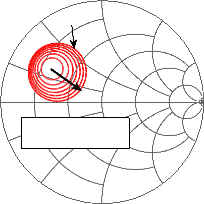
Figure1.For NFmin operation, Different operating gain circles obtained by changing the GP factor in (15)
 Table1.Basic equations used in the analysis
 Γin−Γâˆ-
C1 = |S11 −∆Sâˆ-|(10)

 Γb=S
Γb=S
- GA
1 −ΓinΓS
gA=
2(11)
Γout−Γâˆ-
|S21|

 Γb=L
Γb=L
(2)
g Câˆ-
1 −ΓoutΓL
CP=P 2
(12)
S12S21ΓS
1 + gP(|S22|2 −|∆|2)

 Γin= S11 + 1 −S Γ
(3)
 I
I
P
S12S21ΓS
rP=22

 Γout= S22 + 1 −S Γ
(4)
1 + gP(|S22|
−|∆|)
(13)
SWR= 1 + |Γa|(5)
in1 −|Γa|
C2 = |S22 −∆Sâˆ-|(14)
 GP
GP
SWR= 1 + |Γb|(6)
out1 −|Γb|
gP=
|S21
(15)
|2
GT=
1 −|ΓS|2
|1 −ΓsS11|2
|S21|2
1 −|ΓL|2
|1 −ΓLΓout|2
. (7)
1 −|S11|2 −|S22|2 + |∆|2
 2|S21S12|
(16)
CA=
gACâˆ-
(8)
G= |S21|I2
 1 + gA(|S11|2 −|∆|2)
I
Pmax
|S12
(K−
|
K −1)(17)
 1 −2K|S21S12|gA+ |S12S21|2g2
NF = NFmin+
4rn|ΓS−Γopt|2
(18)
rA=
1 + gP
(|S11
(9)
|2 −|∆|2)
(1 −|ΓS
|2)|1 + Γ
opt|2
-
 (b)
(b)
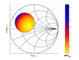
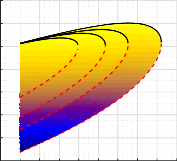
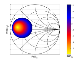
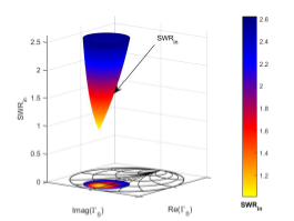
Figure2.Distribution of SWRout over operating gain circles for NFmin operation at 12 GHz a) A 3D representation with small values of SWRout displayed in lighter colors, b) A plane view of the same figure with actual values of SWRout on the color bar.
2.1. Imposing SWR on GT Boundaries for a Wideband, NFmin Operation
Considering the above choices, the bilateral property of the Device Under Test (DUT) disfavor the usage of GT circles. Also, targeting a NFmin operation forces ΓS=Γoptand this prevents the usage of GA circles. As a result, GP circles in the ΓL plane of the Smithchart were used.
 16
16
14

 1212 GHz11 GHz 10 GHz9 GHz
10
8
6
 Maximum attainable G
T
Minimum attainable G
T
2
1212.51313.51414.51515.51616.5
Operating gain (G )
P
Figure3.GT vs. GP, where GTmin ≤GT≤GTmax regions for frequencies 9,10,11,12 GHz are shown in solid and dotted lines respectively.
For a certain frequency of operation, changing the value of the GP factor in (15) will produce different circles for the operating gain as shown in Figure.1. Each point on the circumference of these circles represent a unique value of ΓLthat can be used for matching according to the desired design goals. For further discovery of the device capabilities, SWR related to these values can be imposed on these circles. For illustration, only the SWRout levels are imposed in Figure.2 where lighter color regions represent lower values of SWRout. Although these are the desired regions to build our design around. However, for a wideband operation, reaching the required GT could prevent choosing matching points from these regions.
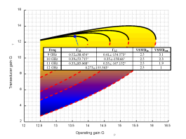
Since ΓS=Γoptfor a NFmin operation, a graphical relation (GT vs. GP) will provide a pre- design information about the limitation of the selected transistor. Figure.3 explains this by specifying GTmin ≤GT≤GTmax over a range of GP for the selected frequency points, the solid lines represent GTmax while the dotted lines correspond to GTmin . In fact a database was constructed for this figure that contain all values of ΓL‘s that correspond to each GP value. Later on, this database will be very useful in choosing appropriate matching points for wideband operation. A quick look to the figure revels that if targeting a wideband operation the desired GT should not exceed GTmax of the highest frequency. For example, the transistor cannot achieve GT higher than 12.73 dB for a selected frequency of 12 GHz.
However, designing for a suitable SWRin and SWRout requires further correlation between GT and SWR. This is shown in Figure.4 where visual predication of the device operating boundaries are clear. The constructed database is extended by masking the contours of both SWRin and SWRout on the GT boundaries at NFmin operation. Since lighter colors indicate better values of SWR, it is obvious that for this particular transistor, the SWRin and SWRout are worse for lower frequencies. Also, the direction of the color stripes are diagonal for SWRin and horizontal for SWRout, this is an indication that, for this particular transistor, choosing an appropriate GP and its subsequent ΓL‘s could result in a constant value of SWRin along the entire bandwidth.
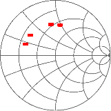
As an example to emphasise on using Figure.3 to design a wideband LNA operating at its NFmin, a targeted 12.7 dB is chosen for illustration in the range of 9-12 GHz. From Figure.4, the color contour reveals that the minimum SWRout=1 corresponding to this GT level belongs to a 12GHz operation. Then, the accompanying ΓLpairs for frequencies 9,10,11,12 GHz are fetched for matching purpose as shown in Figure.5(a). The displayed ΓLpairs on the smith chart of Figure.5(b) were used by ADS to construct matching circuits to verify the expected SWR. the obtained simulation results are listed in Table.2 and compares favourably with those listed in Figure.5(a).


 16351650
1430

 1225
1225
12 GHz 11 GHz 10 GHz 9 GHz
10
20
8
15
14

 12
12
12 GHz
10
8
11 GHz
10 GHz
45
40
35
9 GHz30
25
20
6615
10
10
44
55
2
12 12.5 13 13.5 14 14.5 15 15.5 16 16.5 SWRin
Operating gain G
P
(a)
2
12 12.5 13 13.5 14 14.5 15 15.5 16 16.5 SWRout
Operating gain G
P
(b)
Figure4.Imposing the contours of both SWRin and SWRout on the GT boundaries at NFmin operation,
- for SWRin and b) for SWRout
 +j1.0
+j1.0
+j0.5
+j2.0
+j0.2

 12 GHz
11 GHz 10 GHz
- GHz
+j5.0


 0.0∞
0.0∞
11 GHz
(a)
-j0.2
9 GHz
-j0.5
- GHz
-j1.0
(b)
-j2.0
-j5.0
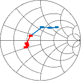
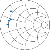
Figure5.a) Extracting the underlying ΓLpairs from the constructed database for the shown selected point of operation according to the targeted GT ans SWR, b) Smithchart representation of the extracted ΓL pairs
- NF BOUNDARIES FOR A UNITY SWROUT
 For the condition of an output conjugate matching (ie. ΓL=Γâˆ-
), GA= GT and a unity SWRout is
produced. All values of ΓSthat corresponds to a particular GA circle gives the same value of SWRin.
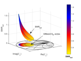
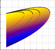
This is shown in Figure.6 where a contour of SWRin is imposed on GA= GT circles. The tip of the cone
 in Figure.6(a) corresponds to ΓSpoint that will produce a simultaneous conjugate match (ie. ΓS=Γâˆ- &
 ΓL=Γâˆ-
) where (SWRin= SWRout=1).However, this figure alone cannot correlate the (GT,NF,SWR)
triplets to give a full visualization insight of the device capability in this case of operation.
- GT, SWRin and NF Correlation for SWRin=1
Figure.7(a) illustrate the variation of SWRin along a range of GA= GT values where at SWRin=1, a simultaneous conjugate matching occurs. The data in Figure.7(a) alongside GA= GT values and their corresponding NF are used to construct a database to help plotting the NF boundaries shown in Figure.7(b). For a SWRout=1 operation, this figure can be used to visually predict both NF and SWRin for any targeted GT. Since, the marked points on the plot represent SWRin=1 for each selected
Table2.ADS simulation data results after individually matching the IMN and OMN according to the matching points in Figure.5(a).
|
Freq |
GT |
NFmin |
NF |
SWRin |
SWRout |
|
9GHz |
12.742 |
0.31 |
0.31 |
2.472 |
3.073 |
|
10GHz |
12.710 |
0.32 |
0.32 |
2.438 |
2.319 |
|
11GHz |
12.751 |
0.33 |
0.33 |
2.434 |
1.869 |
12GHz 12.760 0.34 0.34 2.379 1.033
-
 (b)
(b)
Figure6.3D representation of SWRin over a range of GA=GT circles a) Isometric view, b) Plan view
frequency, it is visually clear that a SWRin= SWRout=1 is impossible for a wideband, flat gain design.

 For a wideband, flat gain operation with SWRout=1.Figure.7(b) reveals that GT flat max=

 GT max 12GHz is the maximum value of GT to attain a flat gain throughout the bandwidth. The
previously constructed database can be used to fetch ΓS, ΓLthat will produce the visually targeted
(GT, SWRout, NF) triplets from Figure.7(b). As an example, a targeted wideband operation (9-12 GHz)
with GT=13.9 dB is chosen for demonstration, Figure.8 present the underlying ΓS, ΓLfor the visually
selected point. this point was selected to give the targeted GT for a simultaneous conjugate matching
at 12 GHz with NF≤1.4 dB. the source and load matching points for the selected frequencies are shown
in Figure.9. Again, ADS was used to verify the estimated (GT, NF, SWR) triplets by constructing individual matching networks using ΓSand ΓLlisted in Figure.8. Table.3 present the simulation results which compares favorably with the visually estimated values.
Table3.ADS simulation data results after individually matching the IMN and OMN according to the matching points in Figure.8.
|
Freq |
GT |
NF |
SWRin |
SWRout |
|
9 GHz |
13.96 |
1.34 |
3.06 |
1.02 |
|
10 GHz |
13.98 |
1.33 |
2.34 |
1.01 |
|
11 GHz |
13.93 |
1.37 |
1.88 |
1.01 |
12GHz 13.95 1.33 1.12 1.03
- CONCLUSION
In this paper, rigorous graphical investigation to explore the selected device capabilities in the NFmin and SWRout=1 cases was presented. For the first case; a set of GT boundary curves and contours can be visually used to explore the expected values of SWRin SWRout for a targeted GT at NFminoperation. While for the second case; NF boundary curves were used to visually predict the NF, SWRin levels for
 6
6
Simultaneous conjugate matching point
10Γ =Γ* , Γ =Γ* , for 9,10,11,12 GHz
 4.5
4.5
5
9 GHz
S in L
out
4
410 GHz
8
3.5
-

 GHz
GHz
3
- GHz
2
1
 6
6
4
2
12 GHz11 GHz 10 GHz 9 GHz
3
2.5
2
1.5
0
11.5 12 12.5 13 13.5 14 14.5 15 15.5 16 16.5
Transducer gain G
T
(a)
0
12.5 13 13.5 14 14.5 15 15.5 16 16.5
Transducer gain G
T
(b)
SWRin
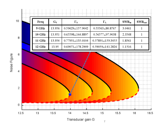 Figure7.a) Distribution of SWRin over a range of GT, b) NF boundaries for frequencies 9, 10, 11, 12 GHz
Figure8.Extracted ΓS, ΓLfrom the constructed database for the shown selected point of operation. output conjugate matching that will result a SWRout=1. For both cases, a full database was formed to
be used in the extraction of the corresponding matching reflection coefficients for any visually targeted
operating points. The construction and using of this database was found to make termination points extraction easy and accurate. And As described by [19] “ItcanbeconcludedthatthenearfuturemicrowavetransistorisexpectedtobeidentifiedbythePerformanceDataBaseswhereallpossibleLNAdesignscanbeoverviewedusingthefulldevicecapacity.“
REFERENCES
- Friis, H.T.,”Noise Figures of Radio Receivers,” Proceedings of the IRE, Vol. 32, No. 7, 419-422, 1944.
- Collins, C.E. et al.,”On the measurement of SSB noise figure using sideband cancellation,” IEEE Transactions on Instrumentation and Measurement, Vol. 45, No. 3, 721-727, 1996.
- Collantes, J.M. et al.,”Effects of DUT mismatch on the noise figure characterization: a comparative analysis of two Y-factor techniques,” IEEE Transactions on Instrumentation and Measurement, Vol. 51, No. 6, 1150-1156, 2002.
 +j1.0
+j1.0
+j1.0
+j0.5
+j2.0
+j0.5
+j2.0
+j0.2
10 GHz
 12 GHz
+j5.0
+j0.2
12 GHz
-


 GHz
GHz
10 GHz
9 GHz
+j5.0
 9 GHz
9 GHz
11 GHz
0.0∞
0.0∞
-j0.2
-j5.0
-j0.2
-j5.0
-j0.5
-j2.0
-j0.5
-j2.0
-j1.0
 -j1.0
-j1.0
(a)
(b)
Figure9.Impedance termination for the numerical example of Figure.8 a) Source impedance matching points b) load Impedance matching points
- Fan, Y. et al.,”Noise power in active broadband metamaterials,” 2013 IEEE Antennas and Propagation Society International Symposium (APSURSI), 1178-1179, 2013.
- Weinreb, S. and Schleeh, J.,”Multiplicative and Additive Low-Frequency Noise in Microwave Transistors,” IEEE Transactions on Microwave Theory and Techniques, Vol. 62, No. 1, 83-91, 2014.
- Fukuda, G. et al.,”Cryogenic GaAs high gain and low-noise amplifier module for radio astronomy,” 2012 Asia Pacific Microwave Conference Proceedings, 905-907, 2012.
- Colangeli, S. et al.,”GaN-Based Robust Low-Noise Amplifiers,” IEEE Transactions on Electron Devices, Vol. 60, No. 10, 3238-3248, 2013.
- Kumar, A. and Pathak, N.P.,”Design and characterization of a wideband p-HEMT low noise amplifier,” 2014 International Conference on Advances in Computing, Communications and Informatics (ICACCI, 785-788, 2014.
- Nosal, Z.M.,”Design of GaAs MMIC transistors for the low-power low noise applications,” 2000 IEEE Radio Frequency Integrated Circuits (RFIC) Symposium, 2000 Digest of Papers, 205-208, 2000.
- Montazeri, S. et al.,”Ultra-Low-Power Cryogenic SiGe Low-Noise Amplifiers: Theory and Demonstration,” IEEE Transactions on Microwave Theory and Techniques, Vol. 64, No. 1, 178-187, 2016.
- [11] Varonen, M. et al.,”An MMIC low-noise amplifier design technique,” 2015 IEEE MTT-S International Microwave Symposium, 1-4, 2015.
- Yarman, B.S. and Carlin, H.J.,”A Simplified Real Frequency Technique Appliable To Broadband Multistage Microwave Amplifiers,” Microwave Symposium Digest, 1982 IEEE MTT-S International, 529-531, 1982.
- Perennec, A. et al.,”Optimization of gain, VSWR and noise of the broadband multistage microwave MMIC amplifier by the real frequency method: synthesis in lumped and distributed elements,” Microwave Symposium Digest, 1990, IEEE MTT-S International, 363-366 vol.1, 1990.
- Capponi, G. et al.,”On the noise-gain performance evaluation of active devices for microwaves,” , Proceedings of the 34th Midwest Symposium on Circuits and Systems, 1991, 418-421 vol.1, 1991.
- Tanzi, N.,”Design of broad-band, low-noise microwave transistor amplifiers with input and output VSWR constraints using CAD tools,” , Proceedings of the 37th Midwest Symposium on Circuits and Systems, 1994, Vol. 2, 1215-1219 vol.2, 1994.
- Bengtsson, O. et al.,”VSWR testing of RF-power GaN transistors,” European Microwave Integrated Circuit Conference (EuMIC), 2014 9th, 460-463, 2014.
- Demirel, S. and Gu¨nes, F.,”Performance characterisation of a microwave transistor for the maximum output power and the required noise,” IET Circuits, Devices Systems, Vol. 7, No. 1, 9-20, 2013.
- Gu¨nes, M. and Gu¨nes, F.,”A new design method for maximum gain formulation of a microwave amplifier subject to noise figure and input VSWR,” Microwave Symposium Digest, 1991, IEEE MTT-S International, 899-902 vol.2, 1991.
- Gu¨nes, F. and Demirel, S.,”Performance characterization of a microwave transistor subject to the noise and matching requirements,” Int J Circ Theor Appl, Vol. 44, No. 5, 1012-1028, 2016.
- Gu¨nes, F. et al.,”A simple and efficient honey bee mating optimization approach to performance characterization of a microwave transistor for the maximum power delivery and required noise,” Int J Numer Model, Vol. 29, No. 1, 4-20, 2016.
- David M., D.M.,”Microwave Engineering,”. 4th ed. Wiley, John Wiley & Sons, Inc., 111 River Street, Hoboken., 2011.
- Gonzalez, G.,”Microwave Transistor Amplifiers: Analysis and Design,”. 2nd ed. Prentice Hall, Upper Saddle River, New Jersey 07458., 1996.
23.
- Renesas Electronics., NEC’s SUPER LOW NOISE HJ FET, NE3210S01 datasheet”( Renesas Electronics ,1999 [Revised August 2015].) .
- Advanced Design Systems (Keysight Technologies, 2009)
- Rollett, J.,”Stability and Power-Gain Invariants of Linear Twoports,” IRE Transactions on Circuit Theory, Vol. 9, No. 1, 29-32, 1962.
- Rollett, J.,”Correction to Stability and Power-Gain Invariants of Linear Twoports,” IEEE Transactions on Circuit Theory, Vol. 10, No. 1, 107-107, 1963.